DESIGN WITH DISCRETE TRANSISTORS

Updated: 1 June 2010
This page provides supplementary information to the chapter on Discrete Design
in my book Small Signal Audio Design. (SSAD)
Back to Home PageBack to The Institute


SOME MORE ON THE 2-TRANSISTOR RIAA PREAMP CONFIGURATION

CONTENTS

INTRODUCTION
Amplifier circuits made with two or three discrete transistors are obsolete if you are looking for the best linearity, as they are easily out-performed by the ubiquitous 5532 in most cases. So why unearth the past? Discrete circuitry may be appropriate when:

  • A load must be driven to higher voltages than an opamp can sustain between the supply rails.
  • A load requires more drive current than an opamp can provide without overheating or current-limiting; eg any audio power amplifier.
  • The best possible noise performance is required. Discrete bipolar transistors can outperform opamps, particularly with low source resistances, say 500 Ohms or less. The commonest examples are moving-coil head amps and microphone preamplifiers. These almost invariably use a discrete input device or devices, with the open-loop gain (for linearity) and load-driving capability provided by an opamp which may itself have fairly humble noise specs.

And two more reasons you might think valid:

  • Aesthetics. If you can get a remarkable performance just from a few discrete devices, I think there is a certain pleasure to be obtained there.
  • Control. Unlike design with op-amps, you have complete control of every voltage, current, and component value in the circuit

THE ORIGINAL CONFIGURATION
The circuit shown in Fig 1 is that given in Small Signal Audio Design. It was deliberately chosen as representative of contemporary practice in its era, and was not modified or optimised in any way. You will note that the single-rail supply is by modern standards low, at +15V; opamp-based preamplifiers would normally run from +/-15V, giving them a 6 dB headroom advantage at once.

Fig 1

The original preamplifier circuit

DC conditions shown

Ic Q1 = 42 uA

Ic Q2 = 0.63 mA

The circuit in Fig 1 is based on a small RIAA preamplifier PCB called the "Lenco VV7", which was intended for upgrading systems to use MM cartridges where the amplifier had only a ceramic pick-up input. It was a Swiss product distributed in Britain by Goldring. It had an integral mains PSU (see the tiny transformer on the left) with half-wave rectification and RC smoothing. What the proximity of that transformer did to the hum levels I do not know, but it looks awfully close to the preamp, which is in the screening can to the right.

I built up the circuit with BC184 transistors, and was not exactly surprised that the performance was mediocre. The THD at 1 Vrms out (1 kHz) was 0.010%, which is a lot for such a low level. The distortion measurement was affected by a high level of hum at the output: -66 dBu at 50 Hz. Carefully screening the whole circuit only reduced this to -68 dBu, so electrostatic pickup was clearly not the major problem.

The RIAA equalisation accuracy is not good, which is only to be expected when you look at the standard component values in the RIAA network. Accurate RIAA networks do not have convenient component values. The errors reach +2.3 dB at 20 Hz and +0.7 dB at 20 kHz; the IEC amendment is apparently not implemented, as it would have given an extra attenuation of -3.0 dB at 20 Hz and -1.0 dB at 40 Hz.

Fig 2

The RIAA error

Pretty gross by today's standards

The preamplifier does not attempt to implement the IEC Amendment; the roll-off below 20 Hz is caused by C3. Increasing it from 47uF to 100uF much reduces the roll-off, as shown by the green trace here.

The preamplifier was being powered from a respectable bench PSU, but it still seemed possible that hum was getting in from the supply rail, as there is absolutely no filtering in the supply to Q1 collector. Inserting a 1K and 22uF filter in the path to R9 dropped the noise output -73.4 dBu. (This figure is the average of six readings, to reduce the tendency of a noise reading to jump about when there is significant low-frequency content. Measurement bandwidth is always 22 -22 kHz unless otherwise stated) A bandpass sweep of the noise output showed that there was now very little extra 50 Hz content. The RC filter gives an attenuation of -16.9 dB at 50 Hz and -22.8 dB at 100 Hz. Increasing the filter capacitance to 100uF however did give a slight improvement, so this was adopted; the attenuation at 50 Hz is now -29.9 dB.
Maximum output with the +15V rail was 3.4 Vrms at 1 kHz, (1% THD) and it is noticeable that clipping is not symmetrical, occurring first on the positive peaks. When this clipping does occur, there is a shift in the DC conditions of the circuit due to the way the biasing works.

Fig 3

THD with a +15V rail, at 1, 2, and 3 Vrms out.

Bandwidth 100Hz-80kHz

Fig 3 shows the distortion performance with a +15V rail, at 1, 2, and 3 Vrms out. (the input level is put through inverse-RIAA equalisation so that the output level remains constant with frequency) It was necessary to use the 100 Hz filter on the AP to get consistent results, despite having got rid of the 50 Hz problem, as there is still a large LF noise component due to the RIAA LF boost.

You can see that for 1 Vrms, things aren't too bad. The mid-band distortion is around 0.01%, but there is a steady rise below 1 kHz. This is caused by the falling feedback factor as the RIAA curve demands more gain at lower frequencies. The other area of concern is at high frequencies; at 1 Vrms nothing too bad happens in the audio band, though THD has reached 0.02% at 20 kHz.
At the higher output level of 2 Vrms, the output stage starts to clip around 15 kHz, as Q2 can no longer drive the RIAA network with its falling impedance at high frequencies. Things are pretty gross at 3 Vrms out, with HF clipping starting at 4 kHz.

Clearly this RIAA preamp could use a bit of improvement. Let's see what can be done with it, concentrating at first on linearity and headroom.

INCREASING THE SUPPLY VOLTAGE TO +24V
The best bet for improving both linearity and headroom is to increase the supply voltage. We will start by turning it up to +24V, a voltage that can conveniently be obtained from a 7824 IC regulator. Fig 4 shows the results; distortion is somewhat reduced overall, and the HF overload problem has been pushed to slightly higher frequencies but the effect is not dramatic. The maximum output is now 3.8 Vrms at 1 kHz, (1% THD)which is not much of a return for increasing the supply voltage by 60%.

Fig 4

THD with a +24V rail, at 1, 2, and 3 Vrms out.

Bandwidth 100Hz-80kHz

Casting a jaundiced eye over the circuit, it's clear that it is still clipping assymmetrically. There is +18.4V on Q2 collector, which is too high for a symmetrical output swing. Rearranging the bias by changing R10 from 3K9 to 2K4 reduces Q2 collector volts to +15.0V, and gives much more output swing; maximum output is now 6.0 Vrms at 1 kHz, an improvement of 4 dB. While this does not give exact symmetry of clipping, it does seem to be close to optimal biasing for linearity. A good indication of this is that the distortion residual at 1 kHz is third-harmonic.
The distortion performance is transformed- 3 Vrms out (1 kHz) gives 0.06% in Fig 4. After re-biasing it has fallen to 0.014%, as in Fig 5. The HF overload effect has also been pushed out to above 20 kHz, even for the 3 Vrms case. Not bad for modifications that essentially cost nothing.

The improvement at lower output voltages is hard to see even with 100 Hz filtering because of the high noise output from a circuit with 50 dB of gain at low but unfiltered frequencies.

Fig 5

THD with a +24V rail, at 1, 2, and 3 Vrms out, after rebiasing.

Bandwidth 100Hz-80kHz

Considerable improvement in both distortion and HF overload behaviour

Fig 6

The story so far.

The RIAA preamplifier using a +24V rail, with the RC filter R6, C12 added to the collector of Q1, and after rebiasing by altering R10.

DC conditions shown

Ic Q1 = 75 uA

Ic Q2 = 1.1 mA

INCREASING THE SUPPLY VOLTAGE TO +30V
Since increasing the supply to +24V gave considerable benefits, we will increase it further to +30V. This increases the maximum output to 6.8 Vrms at 1 kHz, (1% THD) which is 6 dB up on the original circuit. R10 has been changed again to 2K2. The THD for the 1 Vrms case is completely submerged in low-frequency noise, so I used the 400 Hz AP filter, which shows the THD at 1 Vrms 1 kHz is about 0.0055%. This figure however still contains a signficant amount of noise.

Fig 7

THD with a +30V rail, at 1, 2, and 3 Vrms out, rebiased again.

Bandwidth 100Hz-80kHz for 3 and 2 Vrms, 400Hz-80kHz for 1 Vrms

HF overload behaviour has improved again, but HF distortion is rather worse, at all three output levels. The LF distortion is notably improved.

NB This graph is at a slightly larger vertical scale than the previous ones.

As a side issue, we must consider how to generate the supply rail required. The 7824 IC regulator will accept a maximum input of 40V, so it is feasible to use that with the ADJ pin elevated by some means, as described in the SSAD Chapter on power supplies. For voltages above +30V this does not leave enough regulator headroom, and we might need to use the TL783 high-voltage regulator. This is a favourite device for generating +48V supplies for microphone phantom power, and can definitely be relied upon up to this voltage at least.

GAIN DISTRIBUTION IN THE PREAMPLIFIER
At this point I began wondering what else could be done to reduce the distortion. There are practical limits to raising the supply voltage; power dissipation increases, and there is a danger that you could generate turn-on or turn-off transients that would damage stages downstream.

At this point it's worth considering what the sources of non-linearity are. The two transistors, obviously, but the RIAA capacitors could also be contributing, as I used ordinary polyester types, and if you've read the Small Signal Audio Design chapter on components, you will know that these are not wholly linear, and in this application there is a significant signal voltage across them. However the distortion generated by polyester caps is typically of the order of 0.001 % at 10 Vrms, and the signal levels we are using here are much lower than that, so the capacitor contribution is almost certainly negligible. At the time of writing I haven't got round to proving the point by substituting polypropylene capacitors, which are linear.

The configuration looks like cascaded two voltage amplifiers, and it seemed to be a good idea to find out how the open-loop gain is distributed between those two stages. The high value of the Q1 collector load suggests that it might be configured for a high voltage gain.
Measurement showed that the signal on Q1 collector was -49 dB with reference to that on the output at Q2 collector, at 1 kHz. This was confirmed by SPICE simulation, which gave -45 dB on Q1 collector between 100 Hz and 10 kHz. Note however that the emitter of Q2 is connected to AC ground via C3, which suggests that the second stage has a low input impedance and perhaps the first stage is working as a transconductance stage, feeding a current into the base of Q1 rather than a voltage, if you see what I mean. SPICE gives the error voltage, ie that between the base and emitter of Q1 as 38 dB below the output voltage, so the voltage on Q1 collector is less thah that going into the first stage, and this indicates that Q1 is indeed feeding a current to Q2. This is an important finding as it means that the open-loop gain, and hence the feedback factor, cannot be increased by bootstrapping the collector load of Q1, which was the idea I had at the back of my mind all along.

The low-impedance at Q2 base will be further reduced by Miller feedback through the Ccb of Q2, though how significant that is is uncertain at present. Since Cbc is a function of collector voltage this is another potential source of non-linearity.

RUNNING THIS CONFIGURATION FROM DUAL SUPPLY RAILS
The question arises as to how easy it would be to convert this stage to run off dual supply rails, ie +/-V and 0V. The answer appears to be- not very, because the input transistor Q1 that peforms the input-NFB subtraction is sitting very near the bottom rail.

HISTORICAL NOTE- THE DINSDALE MM CIRCUIT
As I stated in Small Signal Audio Design, the first two-transistor MM stage is generally accepted to have been put forward by J. Dinsdale, in an article "Transistor high-quality audio amplifier", in Wireless World for January 1965. This article may be 45 years old but it is still worth reading if you can got hold of it, not least because it discusses how to make an MM preamplifier using just one transistor.
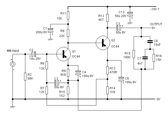
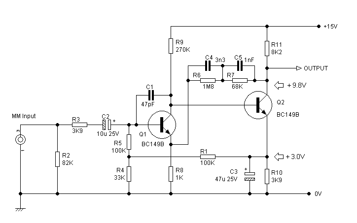
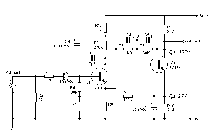
Fig 8

The circuit of the Dinsdale MM stage.

You will note at once that the circuit is upside-down to modern eyes, with a negative supply rail at the top. This was common in circuits of the era, and stemmed from the fact that most germanium transistors were PNP, so if you drew the emitter at the bottom (which is where people were used to drawing valve cathodes) then inevitably you end up with a negative supply rail at the top.
When silicon transistors came in, they were more commonly NPN, so a sigh of relief went up all round as we reverted to the more logical approach of having the most positive rail at the top.

I have not so far tried building this circuit, due to the difficulty of obtaining the transistors.

Comparing this circuit with Figure 1, you can see that there are the characteristic two separate feedback loops, with DC feedback through R13, R14 and R7, and AC feedback to Q1 emitter via the RIAA network R15, C8, R16, C7. Note that the DC path through this network is blocked by C3.

C3 bootstraps R6 to raise the input impedance high enough to give 47K in conjunction with loading resistor R2; disconcertingly Dinsdale refers to this as "feedback" in his article, which it is not.

The OC44 was a PNP germanium transistor made by Mullard. Remarkably, it is still in demand as it is held to give a unique sound in vintage-style fuzz boxes; see www.californiavalveworks.com.

The supply rail voltage is not precisely known, as in the complete preamplifier circuit the MM stage is fed through a network of RC filters that leave the final voltage in some doubt. It clearly is not greater than 20V, judging by the rating of C13, and it seems pretty safe to assume it was around 15V. However the OC44 had a collector breakdown voltage of only 15V, so the rail might have been lower- perhaps 12V.

This circuit uses more parts than the circuit of Figure 1, largely as a result of the different DC bias arrangements. Apart from the transistors, it has 12 resistors and 5 electrolytic capacitors. Figure 1 has (ignoring EMC filtering) 10 resistors and 2 electrolytic capacitors.

Back to Home Page Top of this page Back to The Institute