Much, much, more detail on distortion and other matters
can be found in the new Sixth edition of Audio Power Amplifier Design:

Distortion In Power Amplifiers. |
CLICK BELOW TO GO DIRECT TO SECTION. CLICK ON FIGURES FOR FULL-SIZE VERSION.
1. THE GENERIC AMPLIFIER CONFIGURATION.
Fig 1a shows the generic Lin power amplifier circuit, with the now
universal differential input stage, representing something like 98% of
the amplifiers ever built. It is the obvious starting point for
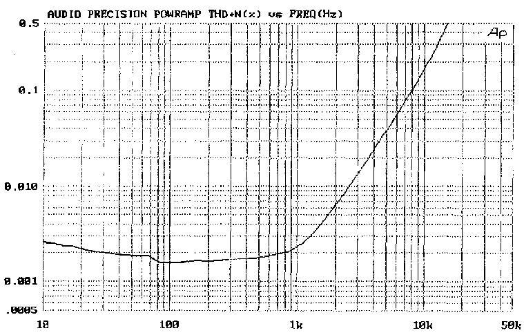
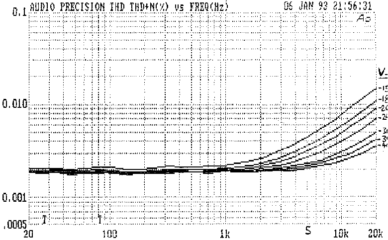
amplifier investigation. [1] Fig 3 shows its distortion plot; there are
two distortion regimes. Below 1 kHz THD is low at 0.002% but not zero,
the noise floor being 0.0006% approx. Above 1 kHz, THD quadruples with
each octave and reaches 0.5% before 20 kHz.
The basic topology is a transconductance amplifier (voltage-
difference input, current output) driving a transimpedance (current-to-
voltage converter) Voltage Amplifier Stage, followed by a unity-gain
power buffer. The voltage at the VAS transistor base is typically only a
couple of millivolts, and is of little interest in itself; it is the
current passed from the input stage to the VAS that counts. This
topology has many advantages, including simple compensation. [2]
2. THE EIGHT DISTORTIONS.
The distortion mechanisms of a generic power amplifier fall into
eight basic categories. Distortion 3 is that generated by the output
stage, subdivided into three different mechanisms 3a, 3b, 3c that are
unrelated in their physical origin. Similarly, Distortion 8 normally
only occurs in the capacitor at the bottom the feedback arm; however, in
AC-coupled designs the output capacitor may contribute significant
distortion.
This classification assumes no clipping, overload, slew-limiting, or
parasitic oscillation.
| SOURCE | ORDER | SLOPE | ORIGIN
| 1 Input stage (balanced) | 3rd-order | 18dB/oct | Inherent
| Input stage (unbalanced) | 2nd-order | 12dB/oct | Inherent
| 2 Voltage Amplifier Stage | 2nd-order | 6dB/oct | Inherent
| 3a Output stage LSN (4 Ohm) | 3rd-order | 6dB/oct | Inherent
| 3b Output stage crossover | Complex | 6dB/oct | Inherent
| 3c Output stage switchoff | Complex | Variable | Inherent
| 4 Non-linear VAS loading | Complex | Flat | Inherent
| 5 Decouple return in ground | Even | Flat | Topological
| 6 Rail induction | Even | 6dB/oct | Topological
| 7 Wrong feedback point | Even | Flat | Topological
| 8 Capacitor non-linearity | Odd | 12dB/oct | Inherent
| .
| |
3. THREE NON-EXISTENT DISTORTIONS. Audio engineering suffers from misinformation, disinformation, and downright lying more than most fields of endeavour. Here are three distortions which either do not exist in detectable quantities or are based on misunderstandings:
3.1 Distortion From The Supply Rails
This is often cited as a serious source of degradation. The only
likely manifestations are Distortion 5 and 6, described below. Providing
these two mechanisms have been suppressed (which is straightforward) and
the amplifier has sufficient power-supply rejection to keep hum and
ripple below the noise floor, then there should be no other way in which
the power supply can degrade linearity.
3.2 Input-Stage Common-Mode Distortion.
This does not appear to exist at detectable levels in normal
amplifier circuitry. It is however true that if an amplifier is operated
at a low closed-loop (C/L) gain such as 1 or 2 times, so there is a
large Common-Mode (CM) voltage on the input stage, distortion at HF is
unexpectedly high, despite the much increased negative-feedback factor.
This distortion is mainly second-harmonic. The immediate cause is the
increased CM voltage on the input devices, but the exact mechanism is at
present unclear. [3] Table 2 shows distortion increasing as C/L gain is
reduced, with output kept constant at 10 V rms. It appears THD is
proportional to CM voltage squared for gain changes.
TABLE 2.
Thus the THD at 1.47 times gain (.00404%) when scaled down for a
realistic C/L gain of 23, is reduced by a factor of (23/1.47)2 = 245,
giving a negligible 0.000017% at 15 kHz.
Closed-Loop Gain 15 kHz THD CM voltage 15 kHz THD
(meas) V rms (calc)
1.00 x .0112% 10.00 .00871% *
1.22 x .00602% 8.20 .00585%
1.47 x .00404% 6.81 .00404% (Ref)
2.00 x .00220% 5.00 .00218%
.
3.3 Thermal Distortion.
Thermal distortion is sometimes described as that caused by cyclic
temperature changes at signal frequency, modulating device parameters.
This is a real problem in ICs, with input and output devices in close
thermal proximity, but in a discrete-component power amplifier there is
no such coupling, and no such distortion.
Thermal distortion would be expected to appear as a rise in second or
third harmonic distortion at very low frequencies, and the largest
effects would be in Class-B output stages where dissipation varies
greatly over a cycle. The effect is wholly absent.
This is probably because drivers and output devices have large
junctions with high thermal inertia. An MJE340 driver transistor has a
chip area four times that of a TL072, so parameters like Vbe presumably
cannot change much even at 10 Hz. The global NFB factor is also highest
at LF. Using my design methodology an amplifier can be straightforwardly
designed to produce less than 0.0006% THD at 10Hz (150W/8-Ohm) without
considering thermal distortion; this suggests that it is not a problem.
THD plots rising at low frequencies are common, but I have always
found the LF rise could be eliminated by correcting either defective
decoupling (Distortion 5) or increasing the feedback capacitor.
(Distortion 8)
As a further argument, consider the distortion residual of an
underbiased Class-B amplifier, using a CFP output so that quiescent bias
depends on the driver temperatures alone. When sinewave power is
delivered to a load, the crossover spikes (generated by the
underbiasing) on the THD residual slowly reduce in height over a couple
of minutes as the drivers warm up. The height of these spikes gives a
continuous indication of driver temperature, and the slow variations
indicate thermal time-constants of tens of seconds, and a negligible
response at 10Hz.
4.1 Open-Loop Gain and Its Measurement.
The closed-loop distortion performance of an amplifier is the product
of open-loop linearity and the negative-feedback factor. For fixed
closed-loop gain, the NFB factor is set by the open-loop gain and its
variations with frequency.
     The open-loop (O/L) gain has two regimes; flat below the lowest pole
frequency P1, (LF) and falling at 6dB/octave above it. (HF)

LF gain is:    LF gain= gm*beta*Rc      	Eqn 1


HF gain is:    HF gain= gm/(w*Cdom)          	Eqn 2


Pole freq is:  P1= 1/(Cdom*beta*Rc)          	Eqn 3


Where:

gm is input stage transconductance.  Beta is VAS current gain.

Rc is VAS collector impedance        w= 2*pi*freq
A typical circuit modification- eg changing the value of R2 in Fig
1a- changes open-loop gain as well as linearity and it is essential to
know if an observed change is due to improved O/L linearity, or simply
increased O/L gain.
Hence the need for a quick and convenient method of measuring O/L
gain. Standard methods for op-amp open-loop gain involve breaking
feedback-loops and manipulating closed-loop (C/L) gains, procedures that
are unlikely to succeed with the average power-amplifier.
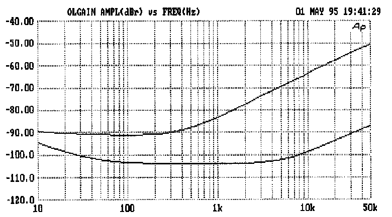
For the generic amplifier in Fig 1, open-loop gain is the output voltage divided by the differential voltage at the inputs. If the C/L frequency response is flat, a plot of open-loop gain versus frequency is obtained by measuring the error-voltage between the inputs, and referring it to the output level. This gives an upside-down plot rising at HF rather than falling, as the amplifier requires more error-voltage for the same output as frequency increases. Fig 2 shows O/L gain of the amplifier in Fig 1.
Given testgear with high CMRR balanced inputs, the method is simple;
buffer the amplifier's differential inputs from cable capacitance with
TL072 voltage-followers, which place negligible loading on the circuit,
and measure the level with respect to the output. The testgear CMRR
defines the maximum open-loop gain measurable; an Audio Precision
System-1 works very well here.
A calibration plot (lower trace in Fig 2)
is produced by feeding the two buffer inputs from the same signal; this
also rises at 6dB/octave, due to testgear input assymmetries, and must
be at least 10dB below the amplifier error signal for accuracy. The
curve flattens out at LF, and may rise, due to imbalance of the testgear
input-blocking capacitors; this makes determination of the lowest pole
P1 difficult, but P1 is not a vital parameter in itself.
4.2 Model Amplifiers.
A linear small-signal section is the obvious starting point for a
low-distortion amplifier; Distortions 1 and 2 can easily dominate
amplifier performance and need to be studied without the complications
of a Class-B output stage. The circuit is reduced to a "model" amplifier
consisting of input stage and VAS only, plus a very linear Class A
emitter-follower as output stage to drive the feedback network; there is
no external loading.
"Model" here means reduced currents rather than voltages. The model
amplifier should be capable of giving a full power-amp voltage swing, as
input-pair distortion depends on absolute output level, and not the
proportion of the rail voltage traversed.
Model amplifiers without slow output stages can give misleadingly
optimistic results for HF stability. A high NFB-factor stable in a model
amplifier can easily be unstable when a real output stage is added. The
value of Cdom should be that anticipated for the complete amplifier.
A typical THD plot from a model amp as in Fig 1 rises with a
steepening slope, as the initial rise at 6dB/octave from the VAS is
contributed to, and then dominated by, the 12dB/octave rise in
distortion from an unbalanced input stage. (see 5.1.2)
4.3 SPICE simulation.
This is a powerful technique; I use PSpice. SPICE gives insight into
the open-loop linearity of both input and output stages, but applying it
to the VAS is problematical as BJT Early Effect is implemented as a
linear approximation. This seems unlikely to give accurate results for a
stage with a large signal on its collector.
5. THE DISTORTION MECHANISMS.
5.1 DISTORTION 1. Input Pair Non-linearity
The input differential pair implements one of the few forms of
distortion cancellation that is truly reliable- the transconductance of
the input pair are determined by transistor physics rather than matching
of variable parameters such as beta. The logarithmic relation between Ic
and Vbe is proverbially accurate over eight or nine decades of collector
current.
The prime motivation for using a differential pair as the input stage
of an amplifier is its low DC offset. Apart from cancellation of the Vbe
voltages, it has the extra advantage that the standing current does not
flow through the feedback network. A second powerful reason, which seems
less well-known, is that linearity is far superior to single-transistor
input stages.
The output current is related to the differential input voltage Vin by:

    Iout= Ie.tanh(-Vin/2Vt)      Eqn 4

    (where Vt is the usual "thermal voltage" of about 26mV at 25 degC,
and Ie the tail current)
Transconductance (gm) is maximal at Vin=0, when the two collector
currents are equal, and this maximum is proportional to the tail current
Ie. [4] Device beta does not figure in the equation, and linearity of the
input pair is not significantly affected by transistor type. The
transconductance plot in Fig 4 shows the linearising effect of local
feedback (emitter degeneration) on the voltage-in/current-out law; it
plots transconductance against input voltage and demonstrates how
emitter degeneration reduces peak transconductance, flattening the curve
over a wider input range. Emitter degeneration markedly improves input
stage linearity, but the overall amplifier NFB factor is reduced, for
the vital HF closed-loop gain is determined solely by input-stage
transconductance and the value of the dominant-pole capacitor. (Eqn 2)
FETs seem a poor idea for the input stage. The basic gm is so low compared with BJTs that there is little scope for linearisation by adding source resistors for local degeneration, so an FET input stage will be very non-linear compared with a BJTs degenerated down to the same transconductance: see 5.1.3.
Curve A in Fig 5 shows the distortion plot for a model amplifier, (5
Vrms output) designed so all distortion is negligible apart from that
from the input stage; with a class A output this simply means ensuring
that the VAS is properly linearised. Note the vanishingly low LF
distortion. For R2 =10K, distortion is below the .001% noise floor until
it emerges at 1 kHz, rising steeply at 12 dB/octave. This rapid increase
is due to the input stage signal current doubling every octave, to feed
Cdom; therefore the associated second harmonic distortion doubles with
each octave increase. Simultaneously the overall NFB available to
linearise this distortion falls at 6dB/octave, and the combined effect
is an quadrupling or 12 dB/octave rise.
If the input stage is properly balanced, only third harmonic is generated, which quadruples rather than
doubling as amplitude doubles, resulting in a 18 dB/octave slope;
however this only appears much further up the frequency range, and the
total distortion produced is much less. If the VAS or output stage
generates distortion it rises at only 6dB/octave, and looks quite
different.
5.1.1 Input stage distortion in isolation.
For serious research we need to measure input-stage non-linearity
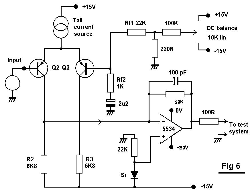
open-loop and in isolation. This is simply done with the test circuit of
Fig 6. The current-to-voltage conversion op-amp uses shunt feedback to
generate an AC virtual-earth at the input-pair output, and uses a third
-30V rail to allow the i/p pair collectors to work at a realistic DC
voltage just above the V- rail; the 10K feedback resistor may be scaled
to prevent op-amp clipping. Input DC balance is set by the 10K pot; the
THD residual diminishes as balance is approached, until the second-
harmonic is nulled, leaving almost pure third harmonic.
5.1.2 Input stage balance.
Exact DC balance of the input differential pair is essential for
minimum distortion. It seems almost unknown that even minor deviations
from equality of collector current (Ic) in the input devices seriously
upset the 2nd-harmonic cancellation, by moving the operating point from
A to say, B, in Fig 4. The gm is both less and changing faster at B, so
imbalance reduces open-loop gain as well as increasing distortion. The
effect of small amounts of Ic imbalance is shown in Fig 7 & Table 3; with
an input of -45dBu an Ic imbalance of only 2% seriously worsens
linearity, THD increasing from 0.10% to 0.16%, while for 10% imbalance
this deteriorates to 0.55%. Ic balance needs an accuracy of 1% or better
for lowest distortion at HF, where the input pair works hardest.
Imbalance in either direction gives similar results.
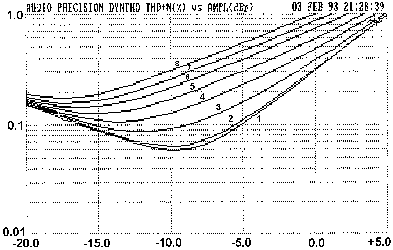
TABLE 3  (Key to Fig 7)

               Curve No.      Ic Imbalance
                    1                0%
                    2              0.5%
                    3              2.2%
                    4              3.6%
                    5              5.4%
                    6              6.9%
                    7              8.5%
                    8               10%

     Imbalance defined as deviation of Ic (per device) from that value
which gives equal Ic in the pair.
This explains the complex distortion changes that accompany the
apparently simple experiment of altering the value of R2. We might
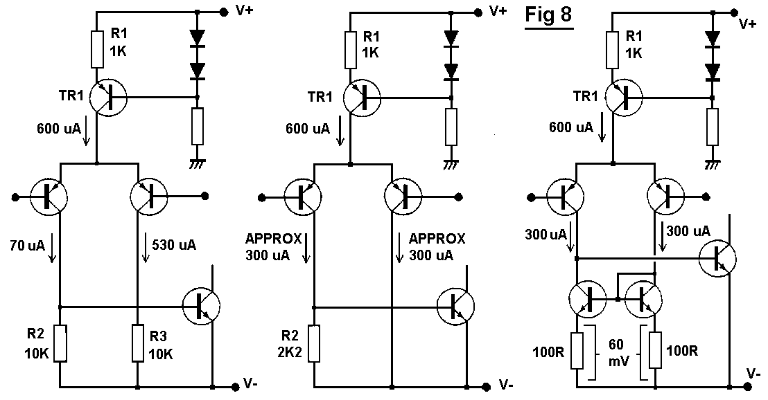
design an input stage as in Fig 8a, where R1 has been selected as 1K by
uninspired guesswork and R2 made high at 10K in a plausible but
misguided attempt to maximise O/L gain by minimising TR2 collector
loading. R3 is also 10K to give the stage a notional "balance";
unhappily this is a visual rather than electrical balance. The asymmetry
is shown in the resulting collector currents; this design generates a
lot of avoidable second harmonic distortion, displayed in the 10K curve
of Fig 5.
Recognising the crucial importance of Ic balance, the circuit can be
rethought as Fig 8b. If the collector currents are to be equal, R2 must
be twice R1, as both have about 0.6V across them. The dramatic effect of
this simple change is shown in the 2K2 curve of Fig 5; the improvement
is accentuated as O/L gain has also increased by some 7 dB, though this
has only a minor effect on the closed-loop linearity compared with the
improved input stage balance. R3 has been removed as it contributes
nothing to input balance.
The input pair can be approximately balanced by the correct values
for R1 and R2, but we remain at the mercy of several circuit tolerances.
The current-mirror configuration in Fig 8c forces the two collector
currents very close to equality when global NFB is applied, giving
excellent cancellation of the second harmonic; the great improvement is
seen in the current-mirror curve of Fig 5. A simple mirror has well-
known Ib errors but they are not large enough to affect distortion.
The hyperbolic-tangent law also holds for the mirrored pair, [5] but
the output current swing is twice as great for the same input voltage.
This doubled output is at the same distortion as a perfectly-balanced
non-mirror input, as linearity depends on the input voltage, which has
not changed. Putting a current-mirror in a well-balanced input stage
therefore increases the total O/L gain by at least 6dB, and possibly by
up to 15dB if the stage was previously poorly balanced; the compensation
by Cdom must allow for this.
Another happy consequence is that slew-rate is roughly doubled, as
the input stage can now source and sink current into Cdom without wasting
some in resistive collector load R2. If Cdom is 100pF, the slew-rate of
Fig 9a is about 2.8V/usec up and down, while 9b gives 5.6V/usec. The
unbalanced pair at Fig 8a displays further vices by giving 0.7V/usec
positive-going and 5V/usec negative-going.

A discrete current-mirror needs its own emitter-degeneration for
accuracy. A voltage-drop across the mirror emitter-resistors of 60mV is
enough to make the effect of Vbe tolerances negligible; without
degeneration there is significant variation in HF THD with different
transistor specimens.
To summarise, the advantages of a mirrored input stage are that
second-harmonic distortion is eliminated, and maximum slew-rate is
doubled.
5.1.3 Improving input-stage linearity.
Even if the input pair has a current-mirror, HF distortion can still
be excessive; once it emerges from the noise floor it octuples with each
doubling of frequency, and so it is well worth postponing the evil day
until as far as possible up the frequency range. Input stage
transconductance increases with Ic, so it is possible to raise gm by
increasing the tail-current, and then reduce it back to its previous
value (otherwise Cdom must be increased to maintain stability) by
applying local NFB in the form of emitter-degeneration. This greatly
improves input linearity, despite its rather unsettling flavour of
something-for-nothing. Input transistor non-linearity can be regarded as
an internal non-linear emitter resistance re, and we have reduced the
value of this (by increasing Ic) and then replaced the missing part with
a linear external resistor Re.
For a single device, the value of the internal re is approximated by:

        re= 25/Ic Ohms   (Ic in mA)          Eqn 5
The original input stage in Fig 1 has a per-device Ic of 600uA,
giving a differential (ie, mirrored) gm of 23 mA/V and re= 41.6 Ohm. The
improved version in Fig 9b has Ic= 1.35mA and so re= 18.6 Ohm; emitter
degeneration resistors of 22 Ohm are added to reduce gm back to its
original value, as 18.6 + 22 is approx 41.6 Ohm. The THD measured by the
circuit of Fig 6 for a -40dBu input voltage falls from 0.32% to 0.032%,
an extremely valuable linearisation which translates into an HF
distortion reduction of about 5 times for a complete Class-B amplifier;
the full advantage is rarely gained. The remaining distortion is still
visually pure third-harmonic if the input pair is balanced.
The reduction of re is limited by the need for practical values of
tail current. As a further benefit, increasing the tail current also
increases slew rate.
5.2 DISTORTION 2
The Voltage-Amplifier Stage (or VAS) is often regarded as a critical
part of a power-amplifier. It provides all the voltage gain and
simultaneously the full output voltage swing. However, as is not
uncommon in audio, all is not quite as it appears. A well-designed VAS
stage contributes relatively little to the total distortion of an
amplifier; if even the simplest steps are taken to linearise it further,
its contribution disappears. This is because the action of Miller
dominant-pole compensation in this stage is rather elegant. It is not
simply a matter of finding the most vulnerable transistor and setting it
in treacle. As frequency rises and Cdom takes effect, negative feedback
is no longer applied globally around the whole amplifier, which would
include the higher poles, but instead is smoothly transferred to a
purely local role in linearising the VAS. Since this stage is
effectively a single transistor, a large amount of local NFB can be
applied to it without stability problems.
VAS distortion arises from the fact that the transfer characteristic of a common-emitter amplifier is curved, being a portion of an exponential. [6] This generates predominantly second-harmonic distortion, which in a closed-loop amplifier will increase at 6dB/octave with frequency. VAS distortion does not worsen for more powerful amplifiers because the stage traverses a constant proportion of its characteristic as the supply-rails are increased. This is not true of the input stage; increasing output swing increases the demands on the transconductance amp as the current to drive Cdom increases.
5.2.1 Measuring VAS distortion in isolation.
Isolating the VAS distortion for study requires the input pair to be
specially linearised, to prevent its steeply-rising distortion
characteristic from swamping the VAS contribution. This is done by
heavily degenerating the input stage; this also reduces open-loop gain,
and the reduced global NFB factor exposes VAS non-linearity. See Fig 10,
where the 6dB/octave slopes suggest an origin in the VAS. Distortion
increases with frequency as Cdom rolls-off the global NFB factor.
To confirm that this distortion is due solely to the VAS, it is
necessary to find a method for experimentally varying VAS linearity
while leaving all other circuit parameters unchanged. In a model
amplifier this can be done simply by varying the V- voltage; this varies
the proportion of its characteristic over which the VAS swings, and thus
only alters the effective VAS linearity, as input stage operation is not
significantly affected. (Fig 10) The Vce of the input devices varies, but
this has negligible effect.
5.2.2 VAS configurations.
Various kinds of VAS are shown in Fig 11. It is important that the
local open-loop gain of the VAS (that inside the local feedback loop
closed by Cdom) be high, to linearise the VAS. Therefore a simple
resistive collector load is unusable. Increasing the value of a
resistive load to increase voltage gain decreases the VAS transistor Ic,
reducing its gm and getting you back where you started.
Local loop gain is enhanced by using an active load to increase the
VAS collector impedance and thus increase the raw voltage gain; either
bootstrapping or a current-source do this effectively, though the
current source is the usual choice. Both active-load techniques have
another important role; ensuring that the VAS can source enough current
to drive the upper half of the output stage. If the VAS collector load
was just a resistor to V+, this capability would be lacking.
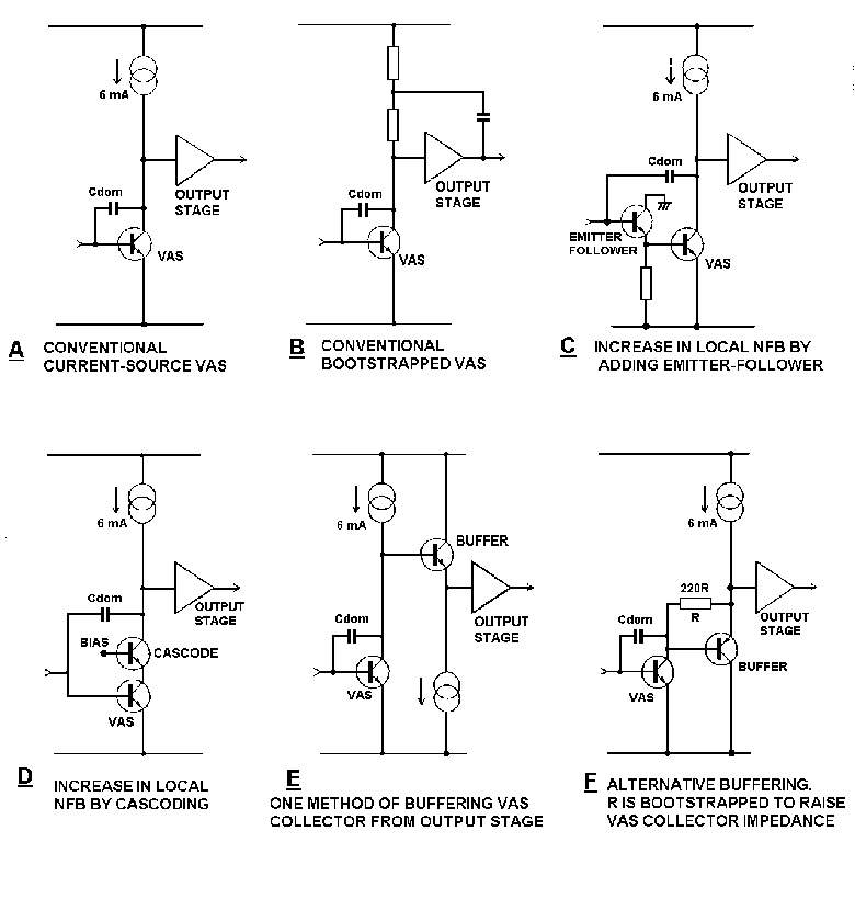
The popular current source VAS is shown in Fig 11a. This works well,
though the collector impedance and hence gain is limited by Early Effect
and output stage loading. It is often stated that this topology provides
current-drive to the output stage; this is not really true. Once the
local NFB loop has been closed by adding Cdom the impedance at the VAS
output falls at 6dB/octave for frequencies above P1. With typical values
the impedance is only a few kohm at 10kHz, and this hardly qualifies as
current-drive.
Fig 11b shows the bootstrapped equivalent. One drawback is that the
increase in voltage gain is determined by the exact gain of the output
stage, which is below unity and varies with loading.
A more dependable form of bootstrapping is available if the amplifier
incorporates a unity-gain buffer between the VAS collector and the
output stage; this is shown in Fig 11f, where R is the VAS collector
load, defining VAS collector current by establishing the Vbe of the
buffer transistor across itself. This voltage is constant, so R is
bootstrapped and appears to the VAS collector as a constant-current
source. A VAS current of 3mA is sufficient, compared with 6mA for the
buffer stage.
5.2.3 VAS enhancements.
The VAS distortion in Fig 10 shows the need for further improvement
over that given by local NFB through Cdom, if our small-signal stages are
to be distortion-free. The virtuous approach might be to try to
straighten out the curved VAS characteristic, but in practice the
simplest method is to increase the amount of local negative feedback
around the VAS through Cdom. Equation 1 shows that LF O/L gain (also the
gain before Cdom is connected) is the product of input stage
transconductance, TR4 beta and the collector impedance Rc. The last two
factors represent the VAS gain and the local NFB can be augmented by
increasing either. So long as Cdom remains the same, the global feedback
factor at HF is unchanged and so stability is not affected.
The effective beta of the VAS can be substantially increased by
adding an emitter-follower. (Fig 11c) Adding an extra stage requires
thought, for if additional phase-shift is introduced, the global loop
stability will suffer. Here the extra stage is inside the Cdom Miller-
loop and so there is little likelihood of trouble from this. The
function of such an emitter-follower is sometimes described as
"buffering the input stage from the VAS" but this is quite wrong; its
true function is VAS linearisation by enhancing local NFB through Cdom.
Alternatively the VAS collector impedance can be further increased to
get more local gain. This can be done with a cascode configuration- (see
Fig 11d) but this technique is only useful when the VAS is not loaded by
a seriously non-linear impedance... such as the input of a Class-B
output stage. See section 5.4. The non-linear loading renders cascoding
largely cosmetic unless a Class-A stage buffers the VAS collector from
the output stage, as in Fig 11e.
When a VAS-buffer is added, the drop in distortion is dramatic, as it
is for the beta-enhancement method. The gain increase is ultimately
limited by Early effect in the cascode and current-source transistors,
and more seriously by the loading effect of the next stage, but it is of
the order of 10 times and gives a useful effect. Fig 12 plots the
distortion of a model amplifier with 100 Ohm input pair degeneration
resistors, showing the extra distortion from a simple VAS. However, the
beta-enhanced version has the THD submerged in the noise floor for most
of the audio band, being well below 0.001%. I think this justifies my
contention that input-stage and VAS distortions need not be problems; we
have all but eliminated Distortions 1 and 2 from the list of eight.
The beta-enhancing emitter-follower is slightly simpler than the
buffered-cascode, but the cost difference is tiny. When wrestling with
these kind of financial decisions it is as well to remember that the
small-signal section of an amplifier usually represents less than 1% of
the total cost, including mains transformer and heatsinks.
Although the two VAS-linearising approaches look very different, the
basic strategy of increased local feedback through Cdom is the same.
Either method linearises the VAS into invisibility.
5.3 DISTORTION 3.
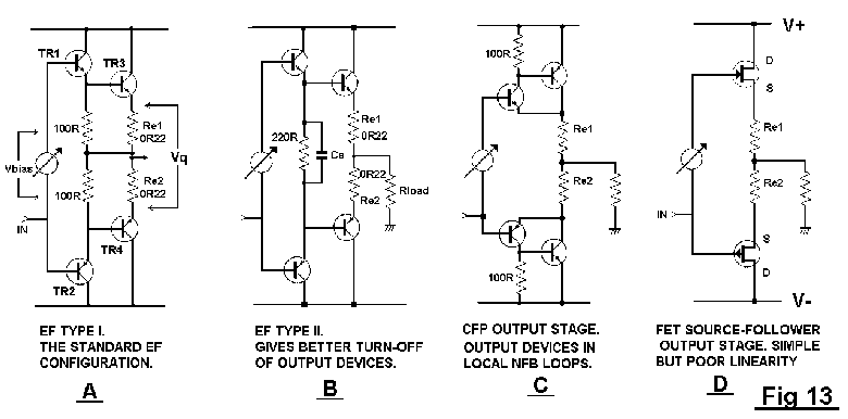
The almost universal choice in semiconductor power amplifiers is a
unity-gain output stage, specifically a voltage-follower. The most
common output stages are shown in Fig 13; two versions of the double-
emitter-follower, (EF) the Complementary Feedback Pair (CFP), and a
source-follower FET output.
The use of power FETs in output stages is often advocated. However, after much investigation, I have found the conclusion inescapable that FETs suffer not only from poor basic linearity, due to low gm, but also a crossover region that is inherently more jagged than BJTs. It is not possible to explore this in detail here, but see [7],[8]
A fundamental factor in determining output-stage distortion is the
Class of operation. Apart from its inherent inefficiency, Class-A is
ideal, having no crossover or switchoff distortion. Distortions 4, 5, 6
and 7 are direct results of Class-B operation and also disappear from a
Class-A design. Distortion 1 (input-stage), Distortion 2 (VAS), and
Distortion 3a (output-stage large-signal non-linearity) remain, however.
Of those Class-A designs which have been published or reviewed, it is
notable that the distortion produced is still significant. This need not
be so; see [9] for a Blameless amplifier biased into Class A, giving THD
below 0.002%, 10 Hz-20 kHz.
It is not generally appreciated that moving into Class-AB, by
increasing the quiescent current, does NOT simply trade efficiency for
linearity. If the output power is above the level at which Class-A
operation can be sustained, THD increases as the bias advances into AB
operation. This is due to so-called "gm-doubling" (ie the voltage-gain
increase caused by both devices conducting simultaneously in the centre
of the output-voltage range, in the Class-A region) putting edges into
the distortion residual that generate high-order harmonics much as
under-biasing does. This vital fact is little known, presumably because
gm-doubling distortion is at a relatively low level and is obscured in
most amplifiers by other distortions.
This is demonstrated in Fig 14a,b,c showing THD residuals for under-
biasing, optimal, and over-biasing of a 150W/8-Ohm amplifier at 1kHz.
All non-linearities except Distortion 3 (output stage) have been
eliminated. The over-biased case had its quiescent current increased
until the gm-doubling edges in the residual had a 1:3 mark/space ratio,
and so was in Class A about one quarter of the time. All three traces
were averaged 64 times to reduce noise; the distortion in 14b is
normally invisible in a 80 kHz measurement bandwidth. The RMS THD
reading for Fig 14a was 0.00151%, for 14b 0.00103%, and for 14c 0.00153%
Spectrum analysis of Fig 14c shows the higher harmonics to be at
least 10dB greater than those for the optimal Class-B case, and
comparable with 14a. In short, Class-AB offers lower distortion than
Class-B below the AB threshold but more above it.
Distortion 3a is the Large-Signal Non-linearity (LSN) that is
produced by in both Class-A and B output stages, ultimately because of
the large current swings in the active devices; in bipolars, but not
FETs, large collector currents reduce beta, leading to drooping gain at
large output excursions. It excludes crossover and switchoff phenomena.
Distortion 3b is classic crossover distortion, resulting from the
non-conjugate nature of the two output halves.
Distortion 3c is switchoff distortion, generated by the output
devices failing to turn off quickly and cleanly at high frequencies, and
is strongly frequency-dependent.
The contributions of 3b and 3c to Distortion 3 occur in Class-B only.
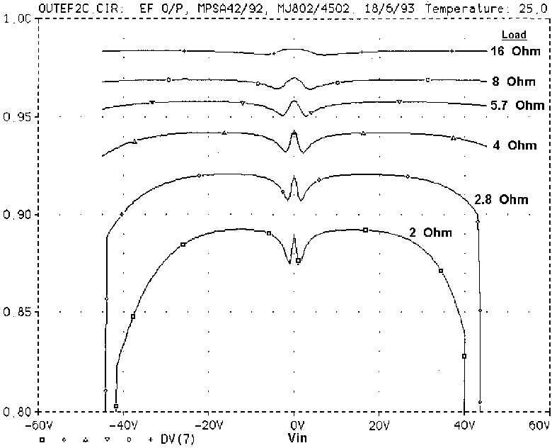
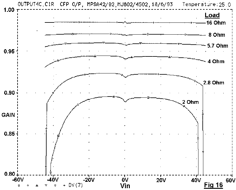
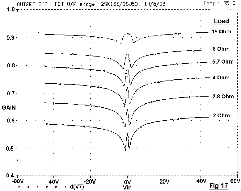
The linearity of the open-loop output stages in Fig 13 with typical values are shown in Figs 15,16,17. These diagrams were generated by SPICE, plotting incremental output gain against output voltage, with load resistance stepped from 16 to 2 Ohms, which I hope is the lowest impedance that feckless loudspeaker designers will throw at us. These plots have come to be known as "wingspread" diagrams, from their birdlike appearance. The power devices were Motorola MJ802 and MJ4502, which are more complementary than many so-called pairs, and minimise distracting large-signal asymmetry. The quiescent conditions are in each case set to minimise peak-to-peak gain deviations in the crossover region for 8-Ohm loading.
The EF output stage.
I have deliberately called this the Emitter-Follower (EF) rather than
Darlington configuration, the latter implying an integrated device with
driver, output, etc in one ill-conceived package. In the EF topology the
input is transferred to the output via two base-emitter junctions in
series, with 100% voltage feedback applied to each device separately to
create cascaded emitter-followers. Fig 13a shows the most prevalent
version (Type I) with driver emitter resistors R1,2 connected to the
output rail. Type II uses one shared resistor Rd, and this improves HF
switchoff; (Fig 13b) basic linearity is the same, see Fig 15. The
crossover region width is approx 10 V, and optimal bias 2.86 V.
.The CFP output stage.
The other major type of bipolar complementary output is the
Complementary Feedback Pair (CFP) or Sziklai Pair, seen in Fig 13c. The
drivers now compare the output voltage with that at the stage input.
Wrapping the outputs in a local NFB loop gives better linearity than EF
versions with 100% feedback applied separately to driver and output
transistors.
The CFP topology is generally considered to show better thermal
stability than the EF, because the Vbe of the output devices is inside
the local NFB loop, and only the driver Vbe affects the quiescent
conditions. The true situation is rather more complex. [10],[11],[12]
The output gain plot is shown in Fig 16; Fourier analysis shows the
CFP generates less than half the LSN of an emitter-follower stage. (See
Table 4) It is hard to see why this topology is not more popular.
The crossover region is much narrower, at about 1V. When under-
biased, this appears on the distortion residual as narrower spikes than
those from an emitter-follower output. Optimal bias here is 1.296V.
TABLE 4.
Fourier analysis of each SPICE gain plot, for 4 and 8 Ohm loading,
yielded these THD % results for a +/-40V input:

        	Emitter          CFP            Simple
	        Follower              		MOSFET

8-Ohm THD      0.031%       	0.014%    	0.47%
Gain:   	0.97		0.97      	0.83

4-Ohm THD      0.042%       	0.030%    	0.84%
Gain: 		0.94       	0.94      	0.72
Combining one of these stages with a distortionless small-signal
section, and applying 30 dB of global NFB, we might expect an amplifier
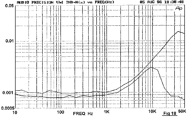
with vanishingly small THD. In fact, crossover distortion remains at HF,
due to the difficulty of linearising high-order distortion with feedback
that reduces with frequency; Fig 18 shows the typical Blameless
performance.
5.3.1 Large-Signal Nonlinearity. (Distortion 3a)
LSN increases as load impedance decreases. In a typical output stage
loaded with 8 Ohms or more, closed-loop LSN is negligible, the THD
residual being almost entirely high-order crossover artifacts that are
reduced less by NFB. As load impedance falls below 8 Ohms, third-
harmonic appears in the residual, and soon dominates. The BJT output
gain plots reveal that LSN is compressive, ie voltage gain falls with
higher outputs.
The fundamental reason for this gain-droop is the fall in output-
transistor beta as Ic increases. [13] In the Emitter-Follower (EF)
topology, beta falloff draws more output-base current from the driver
emitter, pulling driver gain down further from unity; this is the change
in gain that affects the overall transfer ratio. Output-device gain is
not directly affected, as given zero source impedance, beta does not
appear in the equation for emitter-follower gain. As further evidence:
* In SPICE simulation, driving the output bases directly from zero- impedance voltage-sources (rather than drivers) abolishes the gain droop effect. The cause is in the output devices, but the effect is in the drivers.
* The SPICE Gummel-Poon model can be altered so output device beta does not drop with Ic (increase parameter IKF) and once more gain-droop does not occur, with drivers present.
* Measured LSN levels correlate well with the degree of beta-falloff shown in manufacturer's data sheets. This holds for many different BJTs produced over the last 30 years.
LSN does not appear to afflict FET outputs, which have no equivalent beta-falloff mechanism. See Fig 17 where the "wings" of the FET gain plot do not turn downwards at large outputs.
LSN may be reduced in two ways:
* Use output devices that sustain beta well as Ic increases. The 2SC3281 and 2SA1302 transistors (Toshiba, Motorola) show much less beta-droop than average, and 4-Ohm distortion is reduced by about 1.4 times.
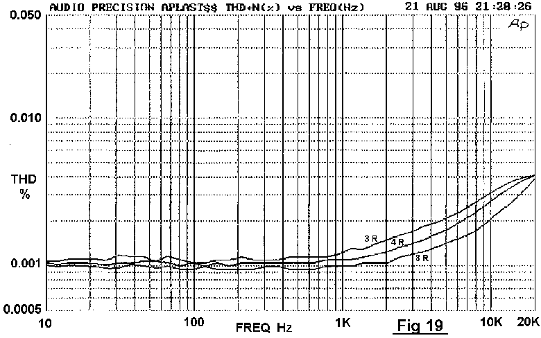
* Use two or more output devices in parallel even though this is unnecessary for handling the power output. Falloff of beta depends on collector current, and if two output devices are connected in parallel, the collector current divides in two between them, and beta-droop is much reduced. Doubling devices reduces distortion by about 1.9 times.
* These two techniques may be combined by using double sustained-beta devices. Doubled device results are shown in Fig 19; distortion at 80W/4 Ohm has halved from 0.009% to 0.0045%. 8 and 4 Ohm traces are now very close, the 4 Ohm THD being only 1.2 times higher.
5.3.2 Crossover distortion. (Distortion 3b)
In a field like Audio where consensus of any sort is rare, it is
widely acknowledged that crossover distortion is the worst problem
afflicting Class-B power amplifiers. The pernicious nature of crossover
distortion is that it occurs over a small part of the transfer
characteristic, and so generates high-order harmonics. Worse still, this
range is around the zero-crossing, so it is present at all levels, the
THD percentage potentially increasing as output level falls, threatening
very poor linearity at low powers.
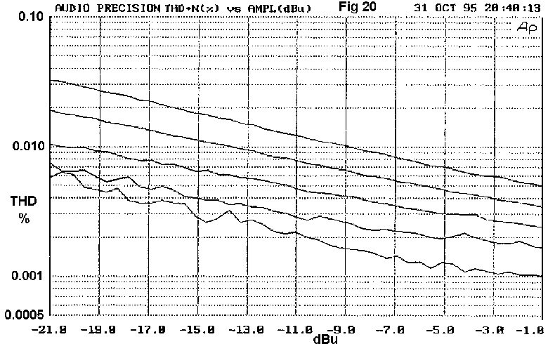
I investigated crossover distortion to see if it really did increase
with decreasing output level in a Blameless amplifier. One problem is
that an optimally-biased Blameless amplifier has such a low level of
distortion at 1 kHz (0.001% or less) that the crossover artifacts are
barely visible in circuit noise, even if low-noise techniques are used.
Thus the THD percentage of the noise-plus-distortion residual is bound
to rise with falling output, for the noise contribution remains
constant; this is the lowest line in Fig 20. To circumvent this, the
amplifier was deliberately underbiased by varying amounts to generate
ample crossover spikes; these upper traces also rise as level falls, but
Fig 20 shows that the THD percentage increases more slowly as level
falls. Both EF and CFP output stages give similar results; whatever the
degree of underbias, THD increases by about 1.6 times as the output
voltage is halved. In other words, reducing the output power from 25 W
to 250 mW, which is pretty drastic, only increases THD % by six times,
and there is no sign of it increasing uncontrollably at low levels.
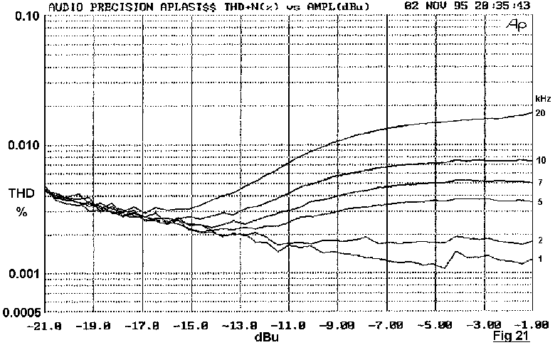
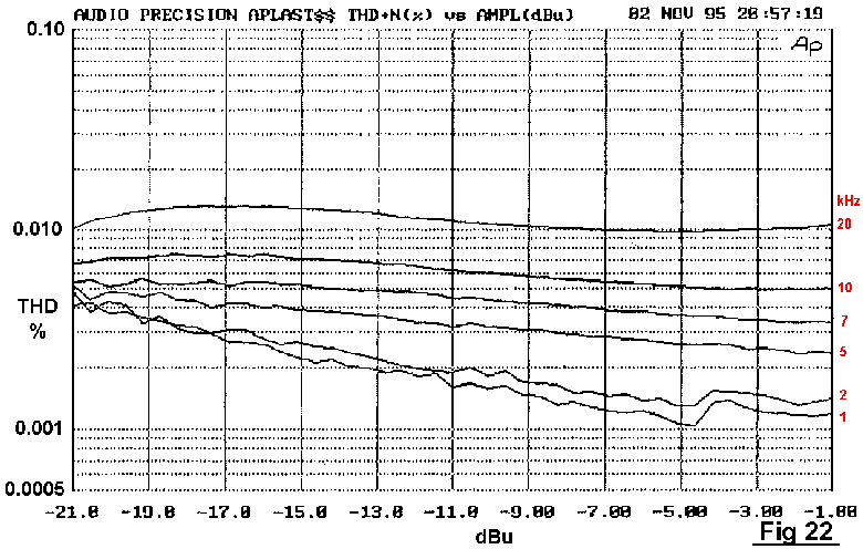
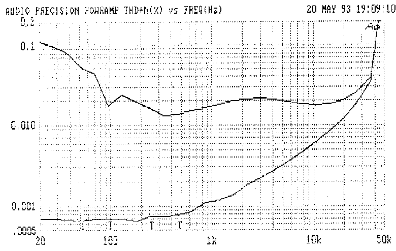
Distortion versus level was also investigated at high frequencies, ie above 1 kHz where there is more THD to measure and optimal biasing can be used. Fig 21 shows THD versus level for the EF stage at a selection of frequencies; Fig 22 shows the same for the CFP. Neither shows a sudden rise in percentage THD with falling level, though it is noticeable that the EF gives a good deal less distortion at lower power levels around 1 W. This is an unexpected observation, and is probably due to the greater width of the EF crossover region.
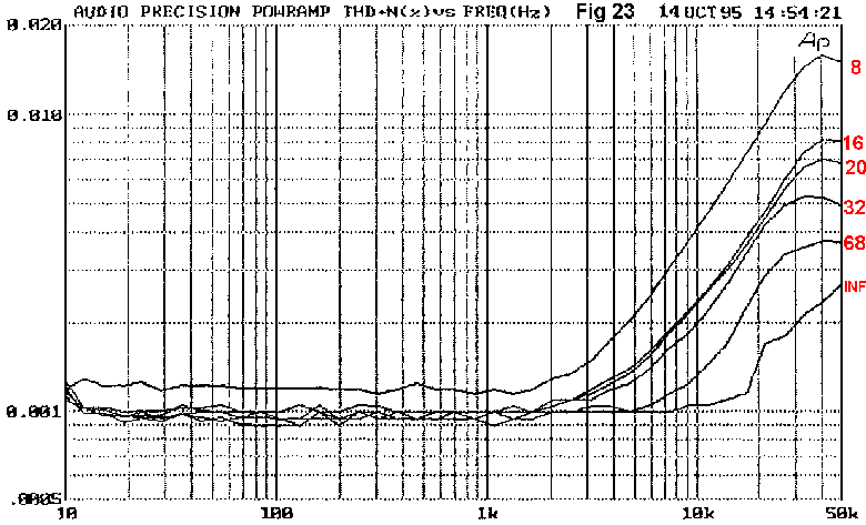
To further get the measure of the problem, Fig 23 shows how HF distortion is greatly reduced by increasing the load resistance, providing further confirmation that almost all the 8 Ohm distortion originates as crossover in the output stage.
The amount of crossover distortion produced depends crucially on
optimal quiescent adjustment, so the thermal compensation used to
stabilise this against changes in ambient temperature and power
dissipation must be accurate. Investigation shows that the critical
parameter is not quiescent current as such, but rather Vq, the quiescent
voltage between the output device emitters; see Fig 13. In both EF and
CFP output stages, changing Re from 0.1 to 0.47 Ohms alters the optimal
Iq considerably, but the values of Vbias and Vq barely change. Thus the
voltage across the transistor base-emitter junctions and Re's is what
counts, not the resulting Iq.
Selecting Re= 0R1 for maximum efficiency is probably the over-riding
consideration. This has the additional benefit that if the stage is
erroneously over-biased into Class AB, the resulting gm-doubling
distortion will only be half as bad as if the more usual 0R22 values had
been used for Re.
5.3.3 Switchoff distortion. (Distortion 3c)
This depends on the speed characteristics of the output devices and
on the output topology. For topologies, the critical factor is whether
the output stage can reverse-bias the output device base-emitter
junctions to maximise the speed at which carriers are swept out, so the
device is turned off quickly. The only conventional configuration that
can reverse-bias the output junctions is the EF Type II, described
below.
The EF Type II configuration in Fig 13b is at first sight merely a
pointless variation on Type I, but its valuable property is that the
shared driver emitter-resistor Rd, with no output-rail connection,
allows the drivers to reverse-bias the base-emitter junction of the
output device being turned off.
Assume that the output voltage is heading downwards through the
crossover region; the current through Re1 has dropped to zero, but that
through Re2 is increasing, giving a voltage-drop across it, so TR4 base
is caused to go more negative to get the output to the right voltage.
This negative excursion is coupled to TR3 base through Rd, and can
reverse bias it by up to -0.5V at 8 Ohms, increasing to -1.6V at 4-Ohms.
Speed-up capacitor Cs improves this action, preventing the charge-suckout
rate being limited by the resistance of Rd. A 1 uF speedup capacitor can
half the THD at 40kHz, implying cleaner switchoff.
The EF Type I has a similar voltage drop across Re2, but the
connection of R1,R2 to the output rail prevents this from reaching TR3
base; instead TR1 base is reverse-biased as the output moves negative.
Charge-storage in the drivers is usually not a problem, so this does
little good. Likewise, a CFP stage can only reverse-bias the driver
bases, and not the outputs.
The second influence on turnoff is the value of the driver emitter or
collector resistors; the lower they are the faster the stored charge can
be removed. Applying these two criteria can reduce HF distortion
markedly, but of equal importance is that it minimises overlap of output
conduction at HF, which if unchecked gives an inefficient and
potentially destructive increase in supply current. [14]
5.4 DISTORTION 4: VAS loading distortion.
Distortion 4 is that which results from the loading of the Voltage
Amplifier Stage (VAS) by the non-linear input impedance of the Class-B
output stage. The VAS collector impedance tends to be high, rendering
it vulnerable to non-linear loading unless buffered or otherwise
protected.
The VAS is routinely (though usually unknowingly) linearised by
applying local negative-feedback via the dominant-pole Miller capacitor,
and this is a powerful argument against any other form of compensation.
If VAS distortion still adds significantly to the amplifier total, then
the local open-loop gain of the VAS stage can be raised to increase the
local feedback factor. The obvious method is to raise the impedance at
the VAS collector, and so the gain, by cascoding. However, if this is
done without buffering the VAS, the loading will render the cascoding
almost completely ineffective. A VAS-buffer eliminates this problem.
The VAS collector impedance, while high at LF compared with other
circuit nodes, falls with frequency as Cdom takes effect, so Distortion
4 is usually only visible at LF. It is also often masked by the increase
in output stage distortion above dominant-pole frequency P1 as the
amount of global NFB reduces.
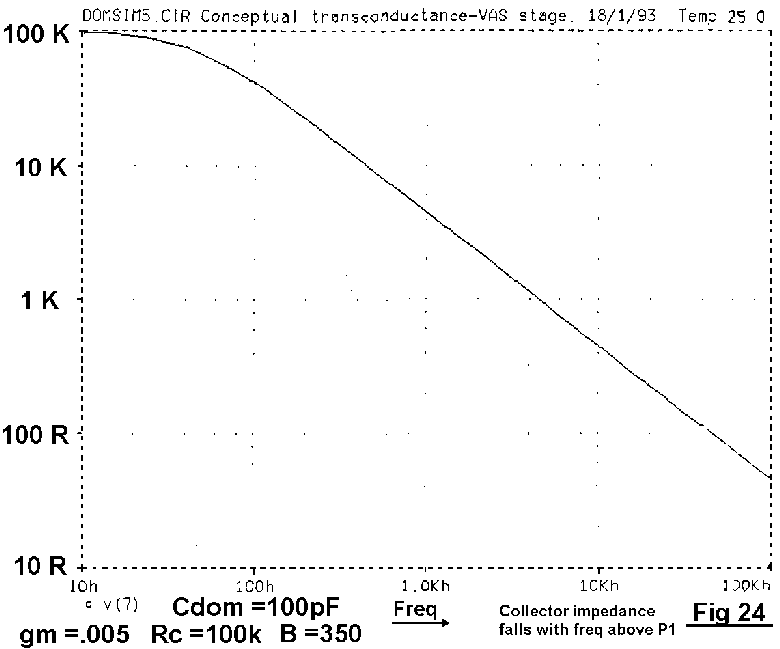
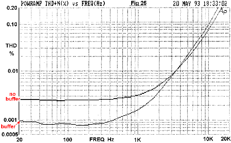
The fall in VAS impedance with frequency is demonstrated in Fig 24, obtained from a SPICE conceptual model.[15] The LF impedance is that of the VAS collector resistance, but halves with each octave above P1. By 3 kHz the impedance is down to 1Kohm, and still falling. Nevertheless, it remains high enough for the input impedance of a Class-B output stage to significantly degrade linearity, the effect being shown in Fig 25.
In [16] it was shown that as an alternative to cascoding, the VAS may
be effectively linearised by adding an emitter-follower within the VAS
local feedback loop, increasing the local NFB factor by raising
effective beta rather than the collector impedance. As well as good VAS
linearity, this establishes a much lower VAS collector impedance across
the audio band, and is much more resistant to Distortion 4 than the
cascode version. VAS buffering is not required, so this method has a
lower component count. The only drawback is a greater tendency to
parasitics near negative clipping, when used with a CFP output stage.
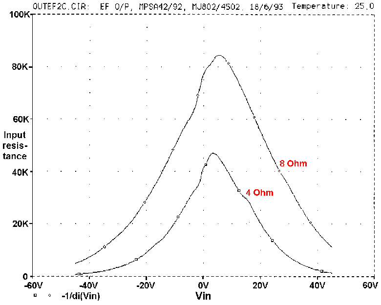
Fig 26 confirms that the input impedance of an optimally-biased EF
Type I output stage is highly non-linear; even with an undemanding 8-Ohm
load, the impedance varies by 10:1 over the output voltage swing. The
Type II EF output has a 50% higher impedance around crossover, but the
variation ratio is greater. CFP output stages have a more complex
variation including a steep drop to below 20 KOhm around the crossover
region.
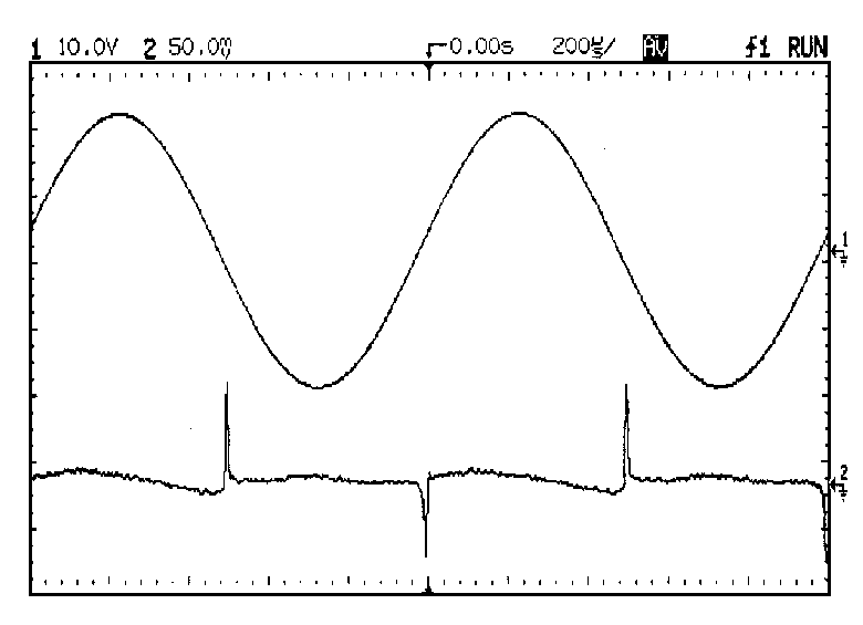
5.5 DISTORTION 5: Decoupling errors.
Most amplifiers incorporate small electrolytics (10 - 220uF) between
each rail and ground to ensure HF stability. As a result rail-voltage
variations cause current to flow into the ground.
If an unregulated power supply is used, (and there are almost
overwhelming reasons for doing so) the rails have non-zero AC impedance
and bear voltage variations due to amplifier load currents as well as
100Hz ripple. In Class-B, the supply-rail currents are halfwave-
rectified sine pulses, and if they contaminate the signal then
distortion is badly degraded. The usual route for intrusion is via
decoupling grounds shared with input or feedback networks, and a
separate decoupler ground back to the star point is usually a complete
cure.(Note that the star-point should be defined on a short spur from the
heavy connection joining the reservoirs; using B as the star point
introduces hum due to the large reservoir-charging current pulses
passing through it)
Fig 27 shows the effect on an otherwise Blameless amplifier handling
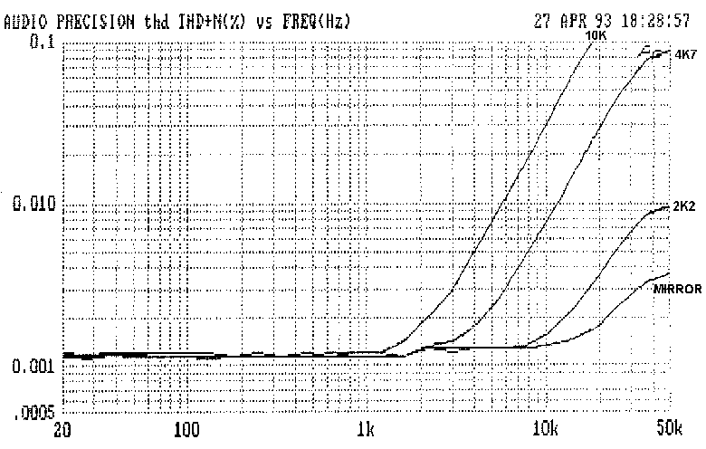
60W/8-Ohm, with 220uF rail decouplers; at 1kHz distortion has increased
by more than ten times, which is quite bad enough. However, at 20Hz the
THD has increased 100-fold, turning a very good amplifier into a
profoundly mediocre one by one misconceived connection.
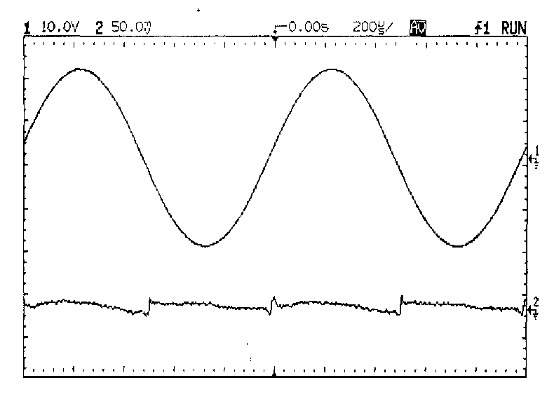
5.6 DISTORTION 6: Induction from supply rails.
Like Distortion 5, this stems directly from the Class-B nature of the
output stage. The supply-rail currents are halfwave-rectified sine
pulses, which can readily crosstalk into sensitive parts of the circuit
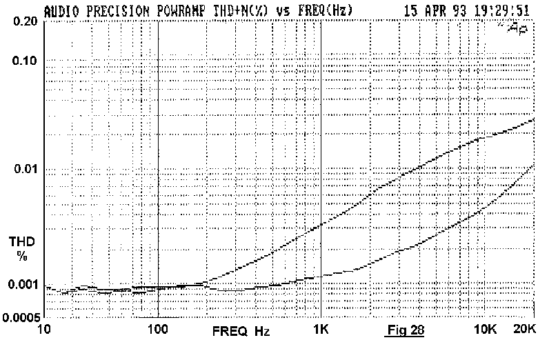
by induction. This is very damaging to the distortion performance; Fig
28 shows a large extra distortion component rising at about 6dB/octave.
The distortion may intrude into the input circuitry, the feedback path,
or even the output cables.
This inductive effect was first publicised by Cherry [17], though the
effect has been recognised by some practitioners for many years.[18]
This effect, apparently unfamiliar to most designers, seems to be a
widespread cause of unnecessary distortion.
The contribution of Distortion 6 can be reduced below the noise
floor. Firstly, rigorously minimise loop areas in the input and feedback
circuitry, ie keep each signal line very close to its ground. Secondly,
limit the ability of the supply wiring to establish magnetic fields in
the first place, by minimising the area of circuit loops carrying half-
wave pulses.
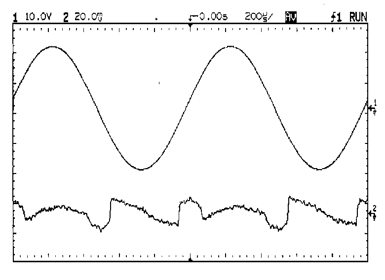
5.7 DISTORTION 7: NFB Takeoff point distortion.
There is a subtle trap in applying global NFB. Class-B output stages
are awash with large halfwave-rectified currents, and if the feedback
takeoff point is in slightly the wrong place, these currents contaminate
the feedback signal, making it an inaccurate representation of the
output voltage, and so introducing distortion; Fig 29 shows the problem.
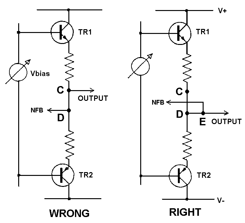
At these current levels, all wires and PCB tracks must be treated as
resistances, and it follows that point C is not at the same potential as
point D whenever TR2 conducts. If feedback is taken from D, then a clean
signal is established here, but the signal at output point C has a half-
wave rectified sinewave added to it, due to the resistance C-D. The
output will be distorted but the feedback loop does nothing about it as
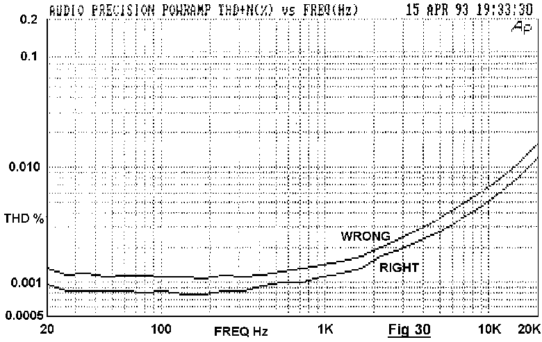
it does not know about the error. Fig 30 shows the practical result for
an amplifier driving 100W into 8-Ohm. The resistive path C-D that did
the damage was a mere 6mm length of heavy-gauge wirewound resistor lead.
To eliminate this distortion is easy, once you are alert to the
danger. Taking the NFB feed from D is not advisable as D is not a
mathematical point, but has a physical extent, inside which the current
distribution is unknown. Point E on the output line is much better, as
half-wave currents do not flow through this arm of the circuit.
5.8 DISTORTION 8: Capacitor distortion.
It seems to be little-known that electrolytic capacitors generate
distortion when they have a significant AC voltage across them. It is
even less well known that non-electrolytics show a similar effect in
applications like Sallen & Key high-pass filters. This has nothing to do
with Subjectivist hypotheses about mysterious non-measurable effects;
this is all too real.
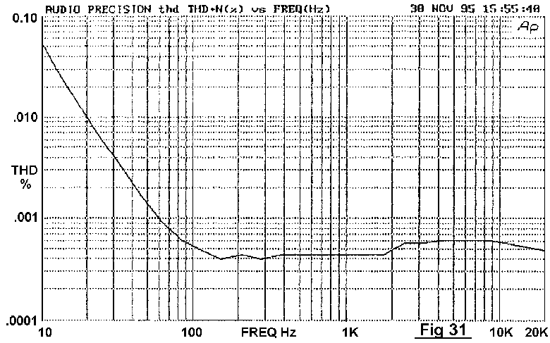
Electrolytic distortion usually arises in DC blocking circuitry with
significant resistive loading. Fig 31 shows the distortion for a 47uF
25V capacitor driving 8 Vrms into a 680 Ohm load. The distortion is a
mixture of second and third harmonic, rising rapidly as frequency falls,
at something between 12 and 18 dB/octave. The great danger of this
mechanism is that serious distortion begins while the response roll-off
has barely begun; here THD reaches 0.01% at 20 Hz when the response is
only down 0.2 dB. The voltage across the capacitor is 2.6 Volts peak,
and this is a better warning of danger than the amount of roll-off. THD
roughly triples as the applied voltage doubles; the factor varies with
capacitor voltage rating.
The mechanism by which capacitors generate this distortion is
unclear. Dielectric absorption appears to be ruled out as this is
invariably modelled by adding linear components to the basic capacitor.
Reverse biasing is not the problem, for DC biasing by up to +15V shows
increased, not reduced distortion. Non-polarised electrolytics show the
same effect but at a much greater AC voltage, typically giving the same
distortion at one-tenth the frequency of a conventional capacitor of the
same value; cost and size generally rules out their use to combat this
effect. The best solution is simply to increase the capacitor value
until the LF distortion remains flat to 10 Hz. A small roll-off in the
audio band is not a sufficient criterion.
While the bandwidth of a system must be defined, using electrolytics
in high-pass filters is never good design practice, because the
tolerances are so large; it is now clear they generate distortion as
well.
Capacitor distortion in DC-coupled power amplifiers is most likely to
occur in the feedback network blocking capacitor. (C2 in Fig 1) The
input capacitor C1 usually feeds a high impedance, but the feedback arm
must have low resistances to minimise noise and DC offset. The feedback
capacitor is thus an electrolytic, and if not quite large enough the THD
shows a characteristic LF rise. Such LF rises are common, but need never
occur. Capacitor distortion is usually the reason, but Distortion 5
(Rail Decoupling Distortion) can also contribute. They can be
distinguished because Distortion 5 typically rises by only 6 dB/octave
as frequency decreases, rather than 12 - 18 dB/octave for capacitor
distortion.
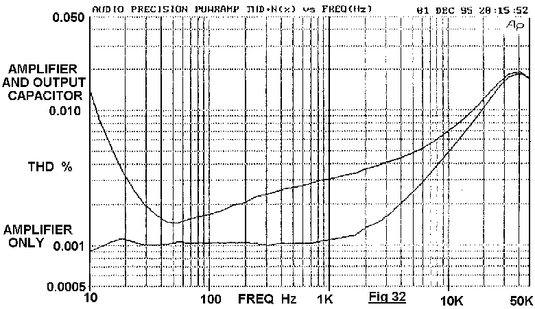
The distortion generated by an AC-coupled amplifier's output
capacitor is more serious, as it is not confined to low frequencies. A
6800uF output capacitor driving 40 W into an 8-Ohm load gives mid-band
third-harmonic distortion at .0025%, as shown in Fig 32. This is five
times more than a Blameless amplifier generates mid-band. Also, the LF
THD rise is much steeper than in the small-signal case.
6: THE BLAMELESS AMPLIFIER CONCEPT.
The basis of the design methodology is really the old clich� "Make
the amplifier as linear as possible before applying Negative Feedback".
In 5.1 and 5.2 it was demonstrated that the distortion from the
small-signal stages can be made negligible compared with output-stage
distortion, by balancing the input pair and adding local negative
feedback to input and VAS stages. Likewise, 5.4 - 5.8 showed that
Distortions 4 to 8 can be effectively eliminated by little-known but
straightforward layout precautions. This leaves Distortion 3, in its
three components, as the only distortion that is in any sense
unavoidable, as Class-B stages free from crossover artifacts are so far
beyond us. This leads to the concept of what I have called a "Blameless
Amplifier", the name being chosen to emphasise that the remarkably low
THD comes from the avoidance of errors rather than from fundamental
advances in circuitry.
A Blameless Amplifier gives a distortion benchmark that varies
relatively little if confined to 8-Ohm loading. It forms a well-defined
point of departure for more ambitious and radical amplifier designs. So
far I have used it as a basis for an extremely linear Class-A design
[9], a Trimodal amplifier (so-called as it operates in any of the modes
A, AB and B, as required) [19], and a Load-Invariant amplifier that
minimises the THD increase with sub-8 Ohm loads.[20]
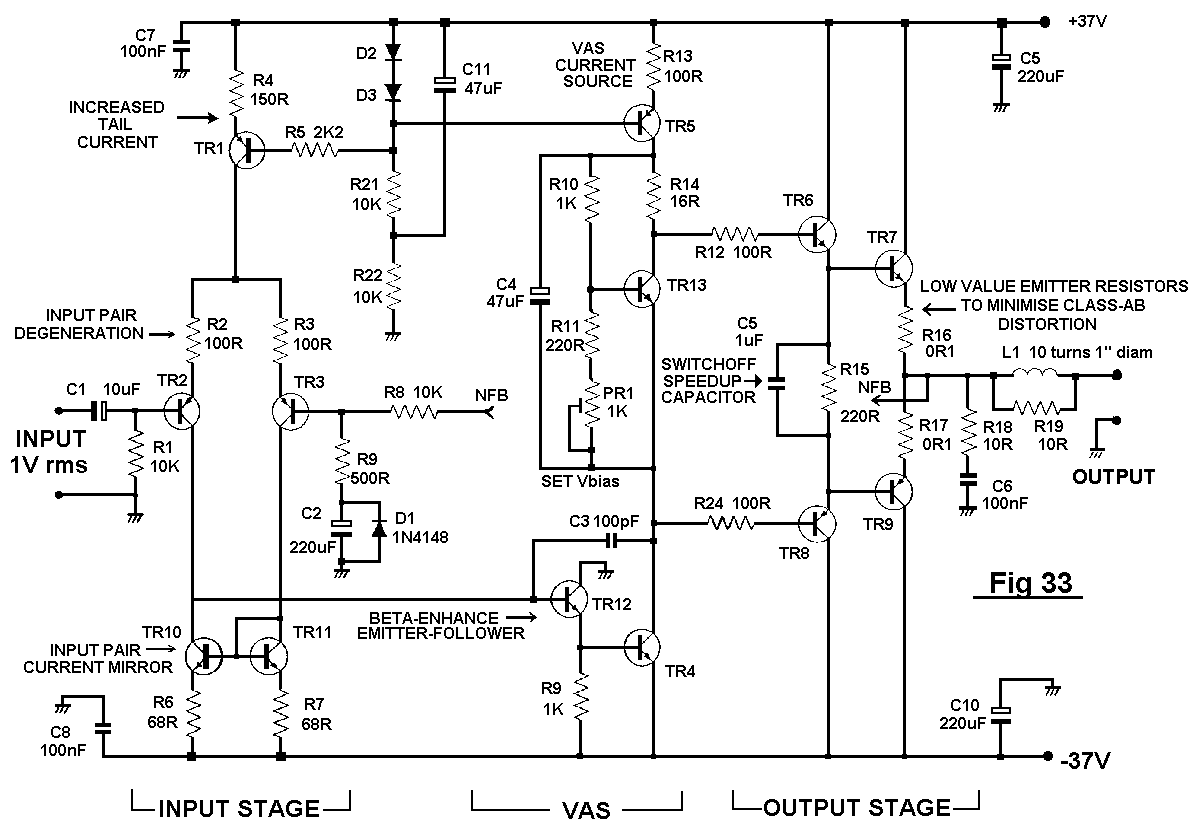
Above: Fig 33 shows the circuit of a Blameless Class-B amplifier.
Note that Fig 33 is only slightly more complex than the standard amplifier in Fig 1.
The input pair now has a current-mirror to ensure input balance, and has undergone constant-gm
degeneration, running at about 3.5 times the tail current of Fig 1. The
VAS is linearised by addition of beta-enhancer TR12, and the remaining
topological distortions were eliminated by careful layout. Performance
is shown in Fig 18.
I am aware that the distortion figures given here are unusually low
for power amplifiers, but I would emphasise they are not freak results
nor dependant on component selection. The only aspect of the linearity
directly affected by device characteristics is distortion below 8 Ohms,
as described in 5.3.1. So far more than twenty thousand 260W/8-Ohm
amplifiers based on the Blameless methodology have been built, with
completely repeatable performance.
CLICK ON PICTURE FOR HIGHER-RES VIEW.
7. CONCLUSIONS.
In this paper I have attempted a concise but complete account of
power amplifier distortion. The linearity obtainable with relatively
conventional circuitry is far better than one would suspect. It also
shows that if power amplifier distortion is to be eradicated entirely,
future work must be focused on the output stage distortions.
If you build a home theater in your house, a high-end power amplifier is a must. While home theater equipment cannot be covered by a home warranty plan, it may be covered by a homeowners insurance policy. A home warranty is different than a homeowners insurance policy, because it covers the costs associated with deterioration or damage of major appliances, as well as the plumbing and electrical systems in your home.If you are interested in home warranty coverage of expensive items (as long as they are shelf products and not self-made) then you can refer to Choice Home Warranty plans and see which one are the best fit for your requirements. |
  
|